We moved! Please visit us at our new home at the University Wuppertal: https://lmo.uni-wuppertal.de/de/

Research
We are a surface science group, working at the intersection between fundamental and applied research. Our main experimental tool is photoelectron spectroscopy, which can be used for example to analyze the position of charge transport level in materials, the composition of surfaces, or the oxidation states of the atoms in a layer. Currently our main focus is on novel semiconductor materials which find application in emerging thin film technologies. Compared to conventional inorganic semiconductors, such as silicon or GaAs, these can be processed using significantly less energy, either by thermal evaporation or solution processing.
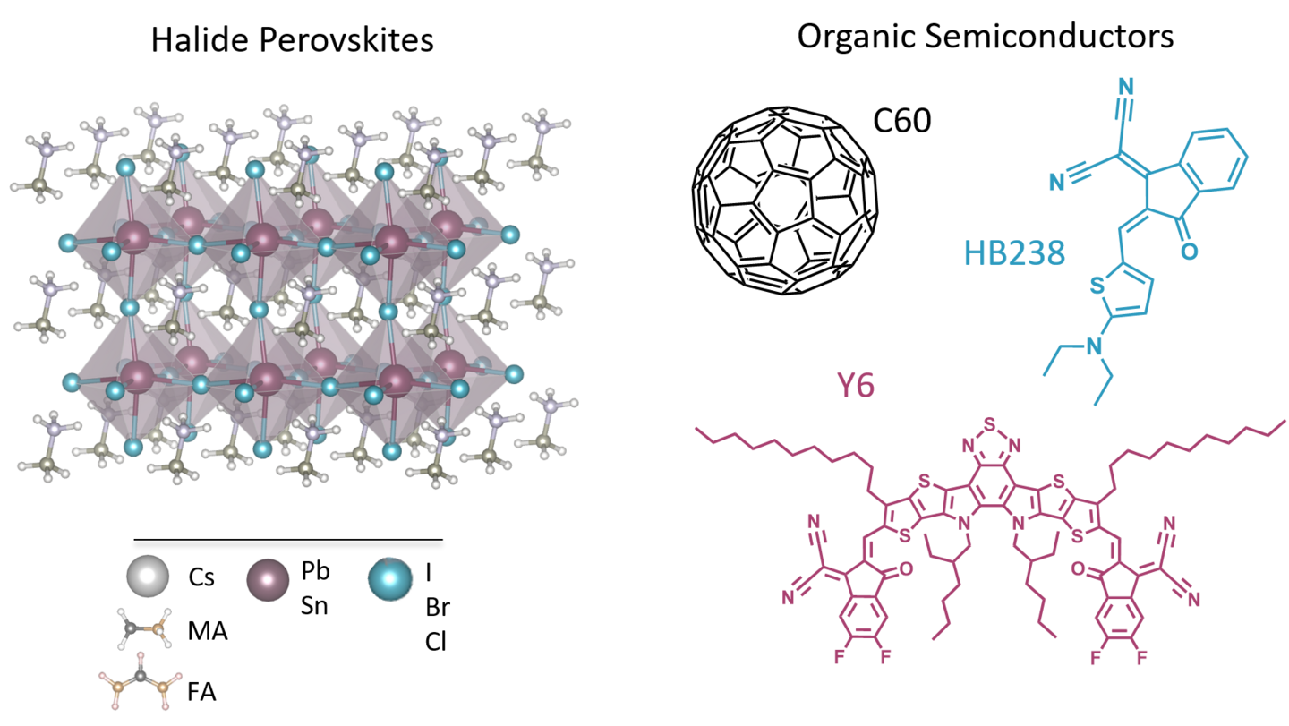
In particular we are working on the two material classes shown below. Organic semiconductors have been extensively researched in the past decades and are composed of carbon-based small molecules or polymers, some examples are shown in the figure below. They are a versatile material class with remarkable potential for low cost optoelectronics due to the processability from solution or by moderate temperature evaporation. The molecular structure of organic semiconductors can be tailored through chemical design, allowing researchers to fine-tune properties such as the energy levels, emission spectra, solubility, or aggregation behavior. The field of halide perovskites, at least with respect to their application in optoelectronic devices, is significantly younger in comparison. The name perovskite refers to a specific crystal structure that can be expressed as AMX3, as shown below. A vast number of such compounds exist in nature, most of which are oxide-based and have insulating properties. But in the last decade, halide-based semiconducting perovskites became of wide-spread interest, in particular when used as absorber material in solar cells. Due to the possibility to combine different atoms or small molecules within this perovskite structure, their (opto)electronic properties are also widely tunable.
In our research we want to gain a better understanding of the fundamental material properties, in particular the energy levels, of these organic and perovskite semiconductors. These values are affected by the choice of material / composition, as well as by processing, post treatment, doping, intermixing etc. To probe these properties, we use UV photoelectron spectroscopy (UPS).
Here, hard UV light is used to excite photo-electrons from a surface. The kinetic energy of these electrons is then measured to extract the initial binding energies, meaning that the occupied density of states and the charge transport levels can be accessed.
By analyzing these properties of materials which are employed in devices such as photovoltaics or light emitting diodes, we can help to gain a better understanding how energy levels and their alignment at interfaces affect the working mechanism of such devices.
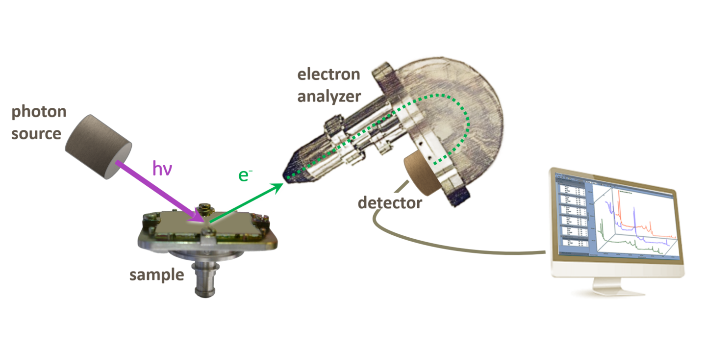
In addition, we employ the related method of x-ray photoelectron spectroscopy (XPS), which predominately probes the more strongly bound core level states of a sample by illumiination with high-energy x-rays. Since these core level signals are element specific and furthermore depend on the atom’s oxidation state, these measurements give insight in the composition of surfaces and the boning environment of its constituents. Lately, we are mostly using XPS to probe chemical interactions that might be going on at interfaces in such thin film devices.