Surface Science Lab
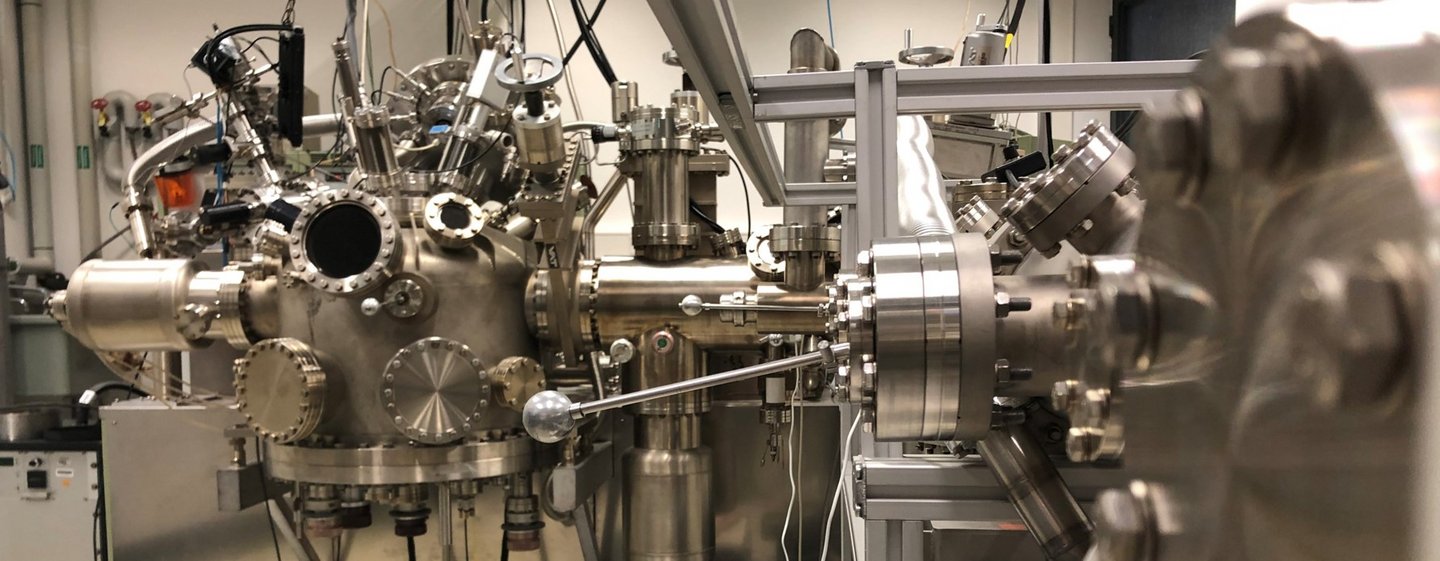

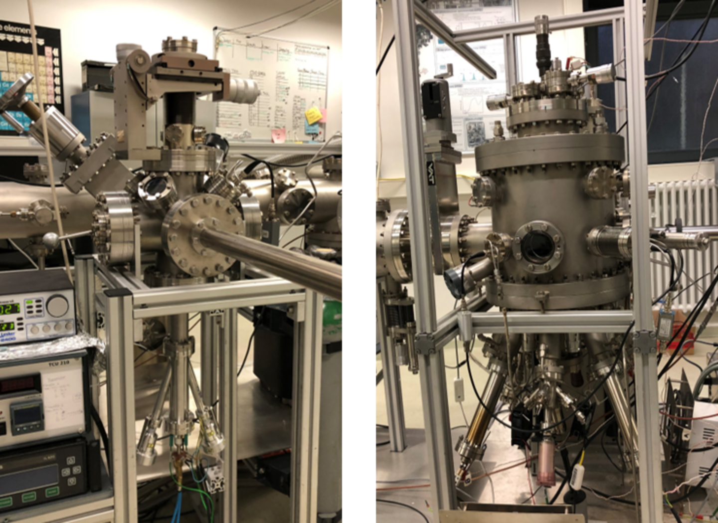
In the Surface Science Laboratory we focus on the investigation of novel semiconducting materials. In our ultra high vacuum cluster tool we can prepare thin films in situ using vapor phase deposition.
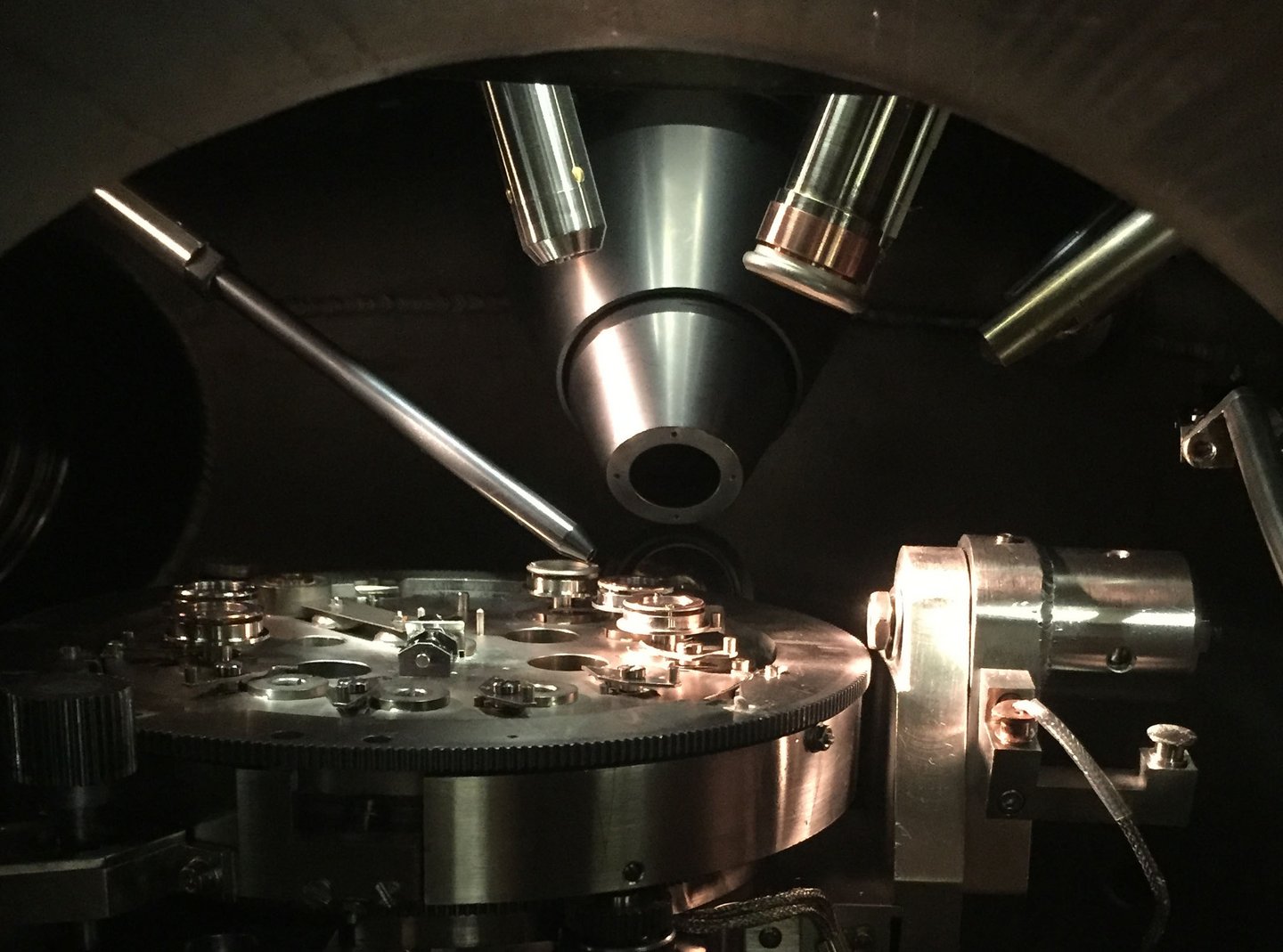
In our evaporation chambers we have two sources for organic semiconductors and 4 sources for perovskite precursors.
Samples can be transferred through vacuum into the measurement chamber
For the characterization we have a variety of methods available
- UPS: UV photoelectron spectroscopy with a monochromized helium source (HeI and HeII),
- IPES: inverse photoelectron spectroscopy with a NaCl/SrF2 bandpass filter
- XPS: X-ray photoelectron spectroscopy using a dual anode Al/Mg source
- REELS: reflection electron energy loss spectroscopy
- LEED: low energy electron diffraction with microchannelplates
- UHV Kelvin Probe